Electron Microscopes: How They Work and the Environment They Need
What an electron microscope is, how SEM and TEM differ, why floor vibration limits real-world resolution, and how DVIA active vibration isolation lets the instrument reach spec.
Last updated
1.What Is an Electron Microscope?
An electron microscope is a microscope that forms images with a beam of accelerated electrons instead of visible light. The change of illumination is not a detail — it is the entire point. Every microscope's resolution is ultimately bounded by the wavelength of whatever it uses to probe the specimen, and visible light has wavelengths of a few hundred nanometers. Features smaller than that blur together no matter how finely an optical microscope's glass lenses are ground. Electrons behave as waves too, and when they are accelerated through a high voltage their effective wavelength becomes many thousands of times shorter than that of light. An instrument built around an electron beam can therefore resolve structures far beyond the reach of light — down to the nanometer and sub-nanometer scale — and deliver useful magnifications of hundreds of thousands of times.
That capability has made electron microscopy a foundational tool wherever structure at the smallest scales matters. Materials scientists use it to study grain boundaries, defects, and coatings; semiconductor engineers rely on it for process control and failure analysis of transistor structures; life-science laboratories image viruses, protein complexes, and cell ultrastructure, with cryo-electron microscopy (cryo-EM) extending the technique to frozen, hydrated biological specimens. Quality control, forensics, and nanotechnology research all lean on the same principle.
The instrument family divides into two main branches — scanning and transmission — which share the electron source and the underlying physics but differ in how the image is formed. Both are examined below, along with the practical question this note builds toward: what it takes to make one perform inside a real building.
2.How Does an Electron Microscope Work?
Strip away the model-specific engineering and every electron microscope is the same functional chain: an electron gun, a set of electromagnetic lenses, a vacuum column, a specimen stage, and one or more detectors.
The electron gun generates the beam. A source — a heated filament or a sharp field-emission tip — releases electrons, and a high accelerating voltage draws them down the column at a controlled energy. The higher the energy, the shorter the electrons' effective wavelength, which is one of the levers designers use to push resolution.
Focusing is done magnetically. Glass is useless to electrons, but a charged particle moving through a magnetic field is deflected, so current-carrying coils around the column — electromagnetic lenses — bend and converge the beam just as curved glass converges light. Because the "lens" is a field generated by a current, focus and magnification are adjusted electronically, by changing currents rather than moving glass.
The entire beam path is held under vacuum. Electrons scatter the moment they meet gas molecules, so pumps evacuate the column from gun to specimen; this is also why samples must tolerate a vacuum environment, or be frozen and protected as in cryo-EM.
Finally, the beam strikes the specimen and produces measurable signals — secondary electrons knocked from the surface, backscattered electrons, X-rays, or electrons transmitted through a thin sample. Detectors convert the chosen signal into an image. Note what this chain implies: the image is carried by charged particles traversing a tall column, so anything that disturbs their flight — a stray magnetic field, a vibrating floor — is written directly into the picture.
3.SEM vs. TEM: What's the Difference?
The scanning electron microscope (SEM) images surfaces. Its lenses condense the beam into a fine probe that is swept across the specimen in a raster, line by line, while detectors count the secondary and backscattered electrons leaving each point. The image is assembled pixel by pixel from that sequence, which gives SEM its characteristic strengths: striking depth of field, three-dimensional-looking surface images, and the capacity to handle bulky samples. Preparation is comparatively light — often no more than mounting the sample and, if it is non-conductive, applying a thin conductive coating.
The transmission electron microscope (TEM) looks through the sample instead. A broad beam passes through a specimen thin enough to be electron-transparent, and the transmitted electrons are projected onto a detector to form the image, revealing internal structure — crystal lattices, interfaces, defects, the interior of cells — at resolutions reaching the atomic scale. The price is preparation: specimens must be thinned to extreme delicacy by mechanical polishing, ion milling, or ultramicrotomy, which makes TEM work slower and more specialized.
Scanning transmission electron microscopy (STEM) combines the two approaches, scanning a finely focused probe across a thin sample and collecting the transmitted signal point by point.
Choosing between them is usually straightforward: surface morphology, fracture analysis, and large samples point to SEM; internal and atomic-scale structure points to TEM. What the two share matters just as much here — both stake their resolution on the stability of a tall column relative to a small specimen, which is why their installation requirements read so similarly.
4.What Actually Limits Resolution in a Real Lab?
Every electron microscope datasheet quotes a resolution figure obtained under ideal conditions — a quiet reference floor, controlled temperature, a benign electromagnetic environment. The number a laboratory actually achieves is set by the installation environment, and the gap between the two can swallow the entire premium paid for a better instrument.
Four environmental factors dominate. Floor vibration moves the specimen relative to the column; because the column is tall, even a microscopic tilt of the supporting platform is levered into a lateral shift at the sample, appearing as blur or as periodic ripple on edges. (Our companion note on vibration isolation for SEM and AFM examines these artifact mechanisms in detail.) Acoustic noise excites panels and the column itself. Stray magnetic fields — from power lines, transformers, or passing elevators — deflect the beam directly. And thermal drift moves everything slowly, smearing long acquisitions.
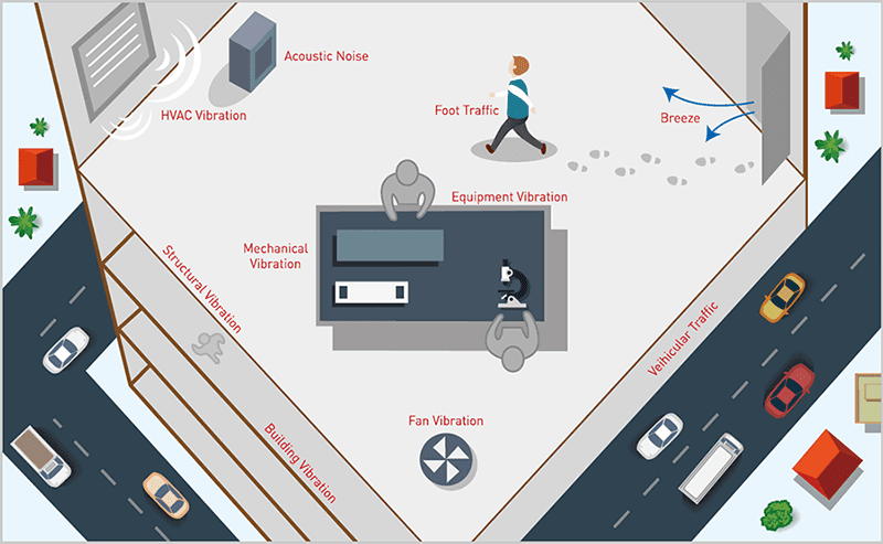
Vibration is usually the most stubborn of the four, because its energy concentrates at low frequency, where buildings are alive: foot traffic, HVAC plant, road traffic, and building sway all deposit their energy below roughly 20 Hz, much of it below 5 Hz. Conventional passive isolators — pneumatic mounts with natural frequencies of 1.2–3.0 Hz — amplify motion near their resonance and isolate well only above roughly 5–10 Hz, so exactly the band where a building moves most is where passive support helps least. Closing that band is the specific role of active vibration isolation, which measures floor motion and cancels it in real time from 0.5 Hz.
5.How Much Vibration Can an Electron Microscope Tolerate?
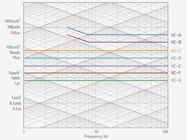
The instrument industry answers this question with the generic vibration criterion (VC) curves, developed by Colin Gordon and his associates and used worldwide to specify how much floor vibration a class of equipment can accept. Each curve sets a limit on RMS velocity measured in one-third-octave frequency bands, and each step down the alphabet halves the allowance: VC-A permits 50 μm/s, VC-C 12.5 μm/s, and so on.
Electron microscopes cluster at the demanding end of the scale. VC-C is the appropriate standard for moderately sensitive electron microscopes working to about 1 μm detail size. VC-D (6.25 μm/s) suits demanding equipment, including many SEMs and TEMs as well as e-beam systems. VC-E (3.12 μm/s) — described as a challenging criterion to achieve — is reserved for the most demanding systems, including e-beam lithography working at nanometer scales. The complete table appears in our vibration criteria note; the microscope vendor's own site-requirement document remains the contractual reference, with VC classes serving as the shared language between facility engineers and instrument makers.
Whether a specific room complies can only be established by a measured floor survey compared band by band against the target curve — our SEM and AFM isolation note covers the survey procedure in detail. That data decides everything that follows.
6.How Do You Prepare a Room for an Electron Microscope?
Room preparation follows a short, strict sequence. First, obtain the microscope maker's site-requirement document — floor vibration limits, magnetic field limits, acoustic limits, floor loading, and clearances. Second, commission a floor survey at the actual proposed footprint and compare it band by band against the required criterion, as described above. Third, check the magnetic and acoustic environment at the same spot. Only then, fourth, select vibration isolation sized to close whatever gap the survey found — chosen from measurement, not from a catalog.
When the survey fails at low frequency — as upper floors and urban sites usually do — an active platform under the microscope is the practical fix. DAEIL SYSTEMS' DVIA-ML, an active system designed specifically for electron microscopes, isolates from 0.5 Hz to 200 Hz, removing up to 80–90% of floor vibration at 1 Hz and up to 90% from 2 Hz upward, in all six degrees of freedom. Because it sits directly beneath the column, it is engineered for electron optics: magnetic emission is held below 0.05 μT, platforms are custom-designed for specific instruments — Krios G4, Glacios 2, and JEM-F200 among them — and capacity reaches 6,000 kg on the DVIA-ML6000, enough for a full cryo-EM column. Where the isolator should form the microscope's base itself, the base-type DVIA-MB applies the same six-axis control; for point support of SEM, TEM, and AFM setups, modular DVIA-ULF isolators install as independent units.
DAEIL SYSTEMS, a vibration isolation specialist since 1984, has published more than 1,000 installation case studies spanning SEM, TEM, AFM, and semiconductor metrology instruments — a record of how consistently this survey-first method converges. The full model lineup and its operating principle are compared on our active vibration isolation systems hub.
| Frequency | Transmissibility (TR) | Residual vibration |
|---|---|---|
| 1 Hz | 0.562 | 56.2% |
| 2 Hz | 0.316 | 31.6% |
| 5 Hz | 0.100 | 10% |
| 10 Hz | 0.100 | 10% |
| 200 Hz | 0.100 | 10% |
DVIA-ML factory acceptance test (FAT) pass criteria, verified on every unit before shipment. Transmissibility is the ratio of platform motion to floor motion; residual vibration is the same figure as a percentage. These are the guaranteed floor, not the typical result: the 80–90% quoted above is what favourable site conditions allow.